Parameters
1×
\( D = \frac{V_{out}}{V_{in}} = \) 0%
\( T_{on} = \frac{D}{f_{sw}} = \) 0 ns
\( T_{off} = \frac{1-D}{f_{sw}} = \) 0 ns
\( \Delta I_{L(pp)} = \frac{(V_{in} - V_{out}) \cdot D}{L \cdot f_{sw}} = \) 0 A (0% of Iout)
Peak Current = 0 A
Valley Current = 0 A
Average Input Current = 0 A
Input RMS Current = 0 A (accounts for ripple and pulsing)
X: - µs, Y: - V
X: - µs, Y: - A
X: - µs, Y: - A
Note: Calculated duty cycle and inductor current assumes ideal components. Closed loop control needed for accurate Vout.
Synchronous Buck Converter Topology
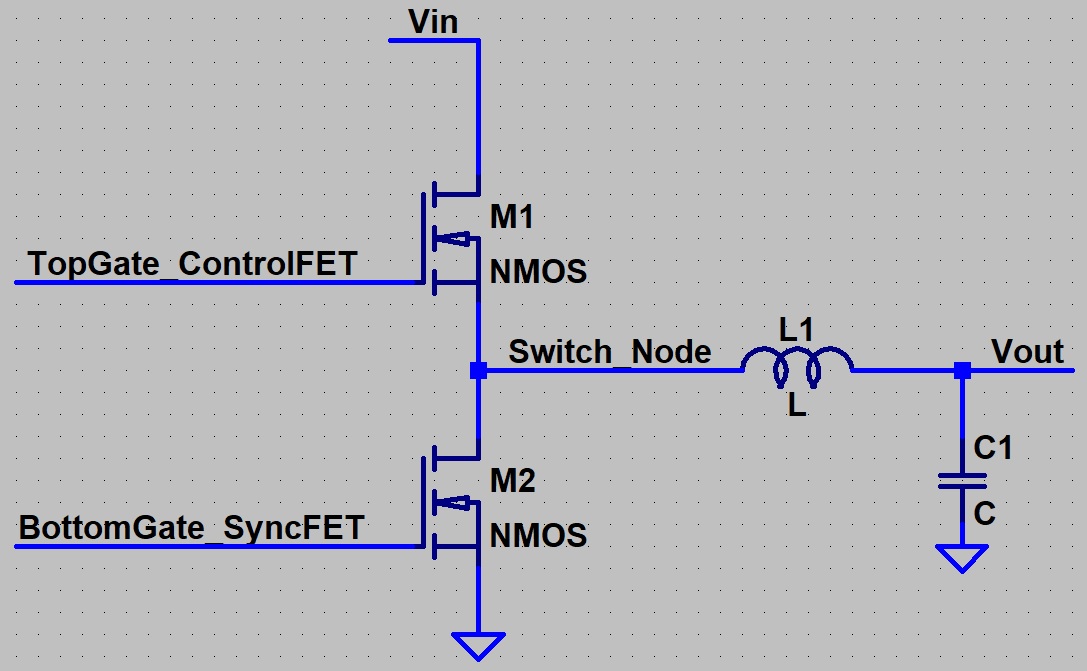
High-side MOSFET (control FET) connects Vin to the switch node during on-time.
Low-side MOSFET (sync FET) provides a low-resistance path during off-time.